VTA Hardware Guide
We present a top-down overview of the VTA hardware design. This hardware design guide covers VTA hardware at two levels:
An architectural overview of the VTA design and its ISA hardware-software interface.
A micro-architectural overview of the VTA hardware modules, and the micro-code specification for the compute core.
VTA Overview
VTA is a generic deep learning accelerator built for fast and efficient dense linear algebra. VTA incorporates a simple RISC-like processor that can perform dense linear algebra operations on rank 1 or 2 tensor registers. In addition the design adopts decoupled access-execute to hide memory access latency.
To a broader extent, VTA can serve as a template deep learning accelerator design for full stack optimization, exposing a generic tensor computation interface to the compiler stack.
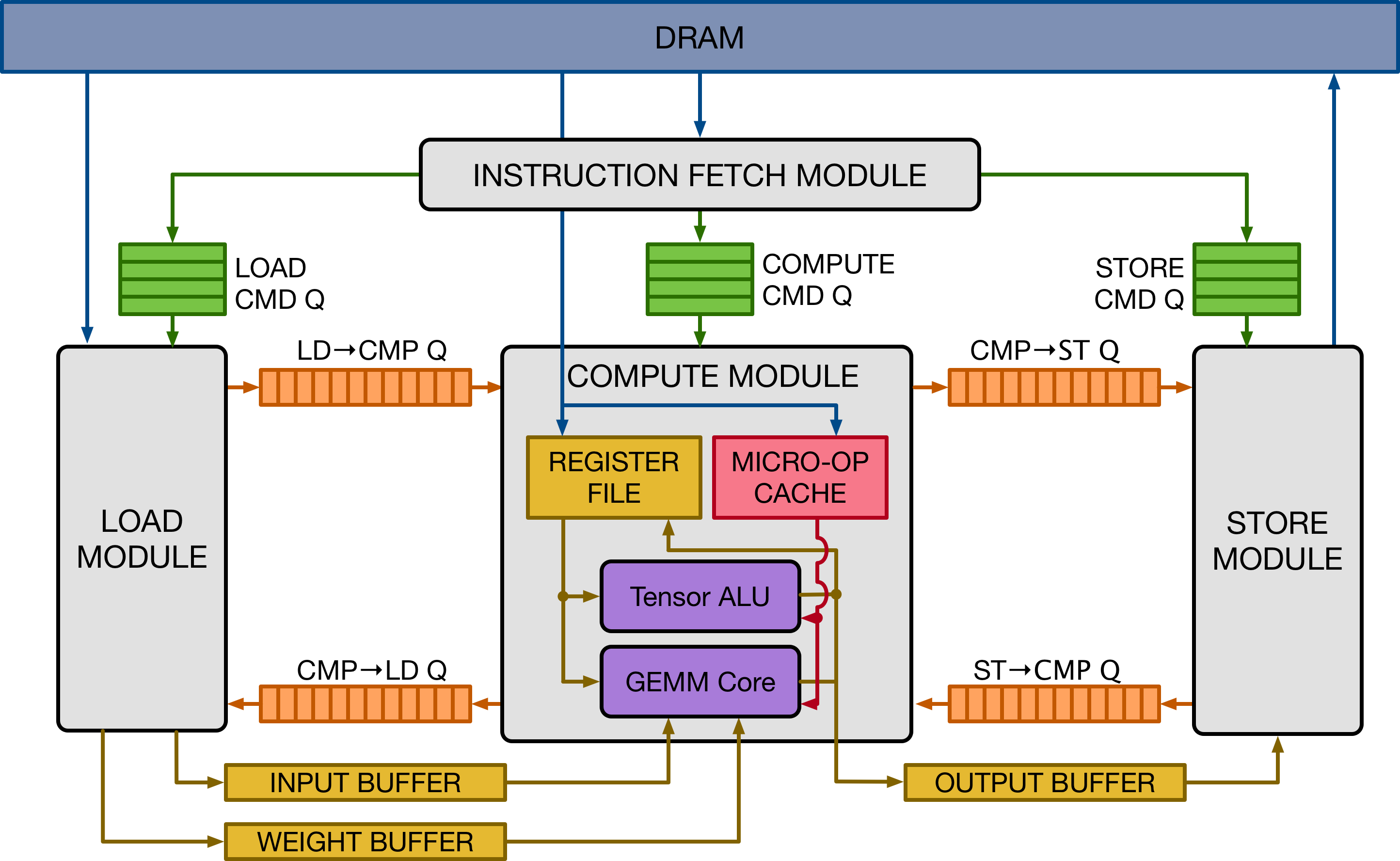
The figure above gives a high-level overview of the VTA hardware organization. VTA is composed of four modules that communicate among each other via FIFO queues and local memory blocks (SRAM), to enable task-level pipeline parallelism:
The fetch module takes care of loading an instruction stream from DRAM. It also decodes those instructions to route them into one of three command queues.
The load module takes care of loading input and weight tensors from DRAM into data-specialized on-chip memories.
The compute module performs both dense linear algebra computation with its GEMM core, and general computation with its tensor ALU. It also takes care of loading data from DRAM into the register file, and loading micro-op kernels into the micro-op cache.
The store module stores results produced by the compute core back to DRAM.
HLS Hardware Source Organization
The VTA design is currently specified in Vivado HLS C++, which is only supported
by Xilinx toolchains.
The VTA hardware sources are contained under 3rdparty/vta-hw/hardware/xilinx/sources:
vta.cccontains the definitions for each VTA module, as well as a top level behavioral model for the top-level VTA design.
vta.hcontains type definitions using Xilinxap_inttypes, and function prototypes declarations.
In addition preprocessor macros are defined under 3rdparty/vta-hw/include/vta/hw_spec.h.
Much of these macro definitions are derived from the parameters listed in the
3rdparty/vta-hw/config/vta_config.json file.
The json file is processed by 3rdparty/vta-hw/config/vta_config.py to produce a string of
compile flags that define the preprocessor macros.
That string is used by the makefile in order to set those high-level
parameters in both the HLS hardware synthesis compiler, and the C++
compiler that builds the VTA runtime.
HLS Module Example
We show a definition of one of the VTA modules defined in C++:
void fetch(
  uint32_t insn_count,
  volatile insn_T *insns,
  hls::stream<insn_T> &load_queue,
  hls::stream<insn_T> &gemm_queue,
  hls::stream<insn_T> &store_queue) {
#pragma HLS INTERFACE s_axilite port = insn_count bundle = CONTROL_BUS
#pragma HLS INTERFACE m_axi port = insns offset = slave bundle = ins_port
#pragma HLS INTERFACE axis port = load_queue
#pragma HLS INTERFACE axis port = gemm_queue
#pragma HLS INTERFACE axis port = store_queue
#pragma HLS INTERFACE s_axilite port = return bundle = CONTROL_BUS

  INSN_DECODE: for (int pc = 0; pc < insn_count; pc++) {
#pragma HLS PIPELINE II = 1
    // Read instruction fields
    insn_T insn = insns[pc];
    // Do some partial decoding
    opcode_T opcode = insn.range(VTA_INSN_MEM_0_1, VTA_INSN_MEM_0_0);
    memop_id_T memory_type = insn.range(VTA_INSN_MEM_5_1, VTA_INSN_MEM_5_0);
    // Push to appropriate instruction queue
    if (opcode == VTA_OPCODE_STORE) {
      store_queue.write(insn);
    } else if (opcode == VTA_OPCODE_LOAD &&
        (memory_type == VTA_MEM_ID_INP || memory_type == VTA_MEM_ID_WGT)) {
      load_queue.write(insn);
    } else {
      gemm_queue.write(insn);
    }
  }
}
- A few observations on HLS coding:
Parameters: The parameter list of each function, combined with the interface pragmas define the hardware interface exposed by the generated hardware module.
Parameters passed by value indicate a read-only hardware memory-mapped register that the host can write to. This fetch function for instance has an
insn_countparameter which will be synthesized as a memory mapped register for the host to write to, in order to set the length of a given VTA instruction sequence.Pointer parameters can mean one of two things depending on the interface pragma being used.
When used with a
m_axiinterface pragma, an AXI requestor interface gets generated to provide DMA access to DRAM.When used with a
braminterface pragma, a BRAM interface gets generated to expose read and/or write ports to an FPGA block-RAM.
HLS streams being passed by reference combined with the
axisinterface pragma produce FIFO interfaces to the module. Hardware FIFOs provide a useful synchronization mechanism between modules.
Pragmas: Compiler pragmas are essential to define hardware implementation of each module. We list several pragmas used in the VTA design to communicate implementation requirements to the compiler.
HLS INTERFACE: specifies the interface of the synthesized hardware module.HLS PIPELINE: defines hardware pipeline performance target by setting an initiation interval goal. When theII == 1target is set, it tells the compiler that the synthesized hardware pipeline should be able to execute one loop iteration per cycle.HLS DEPENDENCE: instructs the compiler to ignore certain types of dependence checks in a given loop. Consider a loop body that writes and reads to the same BRAM structure, and needs to achieve an II of 1. The HLS compiler has to assume worst-case scenario, whereby a read is issued to an address that a past write updated the cycle prior: this cannot be achieved given BRAM timing characteristics (it takes at least 2 cycles to see the updated value). Therefore in order to achieve an II of 1, the dependence checks have to be relaxed. Note that when turning this optimization on, it falls onto the software stack to prevent writes followed by reads to the same address.
Note
This reference guide provides a much more in-depth, and complete specification of HLS for the Xilinx 2018.2 toolchains.
Architectural Overview
Instruction Set Architecture
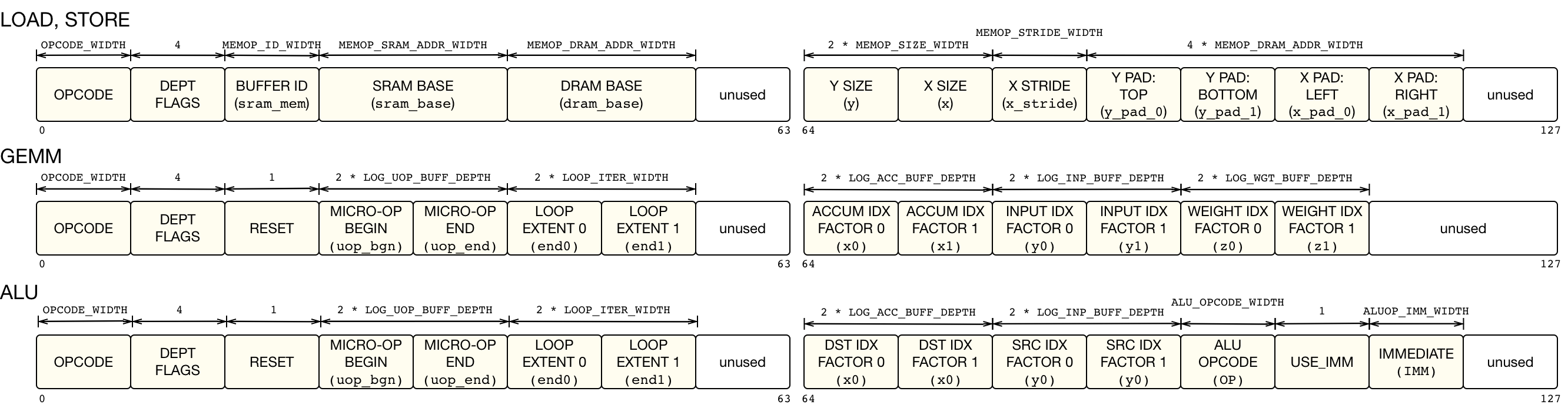
VTA’s instruction set architecture (ISA) is composed of 4 CISC instructions that have a variable execution latency, two of which execute a micro-coded instruction sequence to perform computation.
The VTA instructions are listed below:
LOADinstruction: loads a 2D tensor from DRAM into the input buffer, weight buffer, or register file. It can also load a micro-kernel into the micro-op cache. Supports dynamic padding when loading input and weight tiles.GEMMinstruction: performs a micro-op sequence of matrix-matrix multiplications over an input tensor and a weight tensors, and adds the result to a register-file tensor.ALUinstruction: performs a micro-op sequence of matrix-matrix ALU operations over register-file tensor data.STOREinstruction: stores a 2D tensor from the output buffer to DRAM.
The LOAD instructions are executed by the load and compute modules depending on the store memory buffer location target.
The GEMM and ALU instructions are executed by the compute module’s GEMM core and tensor ALU.
Finally, the STORE instructions are executed by the store module exclusively.
The fields of each instruction is described in the figure below.
The meaning of each field will be further explained in the Microarchitectural Overview section.
Note
Note that the VTA ISA changes as VTA’s architectural parameters are modified (i.e. GEMM core shape, data type, memory size etc.), and as a result the ISA does not guarantee compatibility across all variants of VTA. This is acceptable however, since the VTA runtime adapts to parameter changes, and produces binary code tailored for the version of the accelerator that gets generated. This exemplifies the co-design philosophy adopted by the VTA stack which embraces fluidity of the hardware-software interface.
Dataflow Execution
VTA relies on dependence FIFO queues between hardware modules to synchronize the execution of concurrent tasks. The figure below shows how a given hardware module can execute concurrently from its producer and consumer modules in a dataflow fashion through the use of dependence FIFO queues, and single-reader/single-writer SRAM buffers. Each module is connected to its consumer and producer via read-after-write (RAW) and write-after-read (WAR) dependence queues.
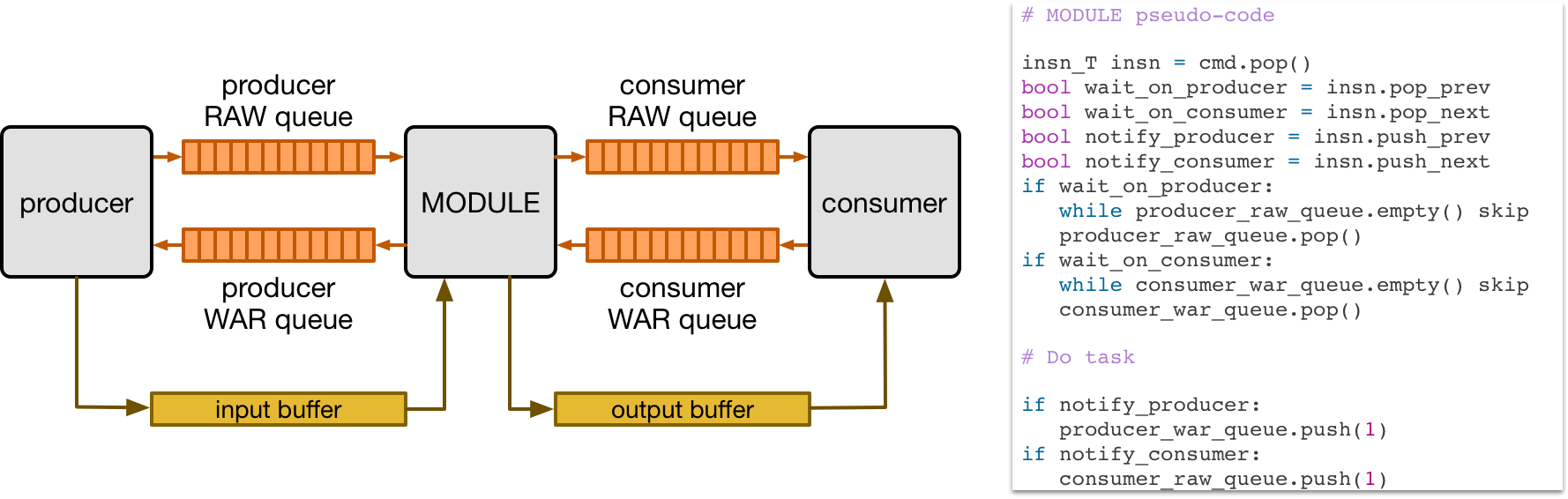
The pseudo-code above describes how a module executes a given instruction predicated on dependences with other instructions. First, the dependence flags within each instruction are decoded in hardware. If the instruction has an incoming RAW dependences, execution is predicated upon receiving a RAW dependence token from the producer module. Similarly, if the task has an incoming WAR dependence, execution is predicated upon receiving a WAR dependence token from the consumer module. Finally when the task is done, we check for outgoing RAW and WAR dependences, and notify the consumer and producer modules respectively.
Note
Note that the dependence tokens in this scenario are information-less. This is because the instructions executed by each module cannot be reordered by design, as they arrive in FIFO order.
Pipeline Expandability
The default VTA design is composed of four modules that describe a 3-stage load-compute-store task pipeline.
Following the dataflow hardware organization principle, we can extend VTA the pipeline to include more stages.
For example, we can envision separating the tensor ALU from the GEMM core in order to maximize the utilization of the GEMM core.
This would result in a load-gemm-activate-store task pipeline which closely reflects the TPU design.
Adding more stages has a cost however: it can add storage and extra logic overhead, which is why we opted for a default 3-stage pipeline.
Microarchitectural Overview
We describe the modules that compose the VTA design.
The module definitions are contained in 3rdparty/vta-hw/hardware/xilinx/sources/vta.cc.
Fetch Module
VTA is programmed by a linear instruction stream. The fetch module is the entry point of VTA to the CPU and is programmed via three memory mapped registers:
The read-write
controlregister starts the fetch module, and is read to check for its completion.The write-only
insn_countregister sets the number of instructions to execute.The write-only
insnsregister sets the start address of the instruction stream in DRAM.
The CPU prepares the instruction stream in DRAM in a physically-contiguous buffer prepared by the VTA runtime.
When the instruction stream is ready, the CPU writes the start physical address into the insns register, the length of the instruction stream into the insn_count register, and asserts the start signal in the control register.
This procedure starts VTA, which reads in the instruction stream from DRAM via DMA.
Upon accessing the instruction stream, the fetch module partially decodes instructions, and pushes those instructions into command queues that feed into the load, compute, and store modules:
STOREinstructions are pushed to the store command queue to be processed by the store module.GEMMandALUinstructions are pushed to the compute command queue to be processed by the compute module.LOADinstructions that describe a load operation of micro-op kernels or register file data are pushed to the compute command queue to be processed by the compute module.LOADinstructions that describe a load operation of input or weight data are pushed to the load command queue to be processed by the load module.
When one of the command queues becomes full, the fetch module stalls until the queue is not full.
Consequently, the command queues are sized to be deep enough to allow for a wide execution window, and allow multiple tasks to be in flight concurrently across the load-compute-store pipeline.
Compute Module
VTA’s compute module acts as a RISC processor that performs computation on tensor registers rather than scalar registers. Two functional units mutate the register file: the tensor ALU, and the GEMM core.
The compute module executes RISC micro-ops from the micro-op cache. There are two types of compute micro-ops: ALU and GEMM operations. To minimize the footprint of micro-op kernels, while avoiding the need for control-flow instructions such as conditional jumps, the compute module executes micro-op sequences inside a two-level nested loop that computes the location of each tensor register location via an affine function. This compression approach helps reduce the micro-kernel instruction footprint, and applies to both matrix multiplication and 2D convolution, commonly found in neural network operators.
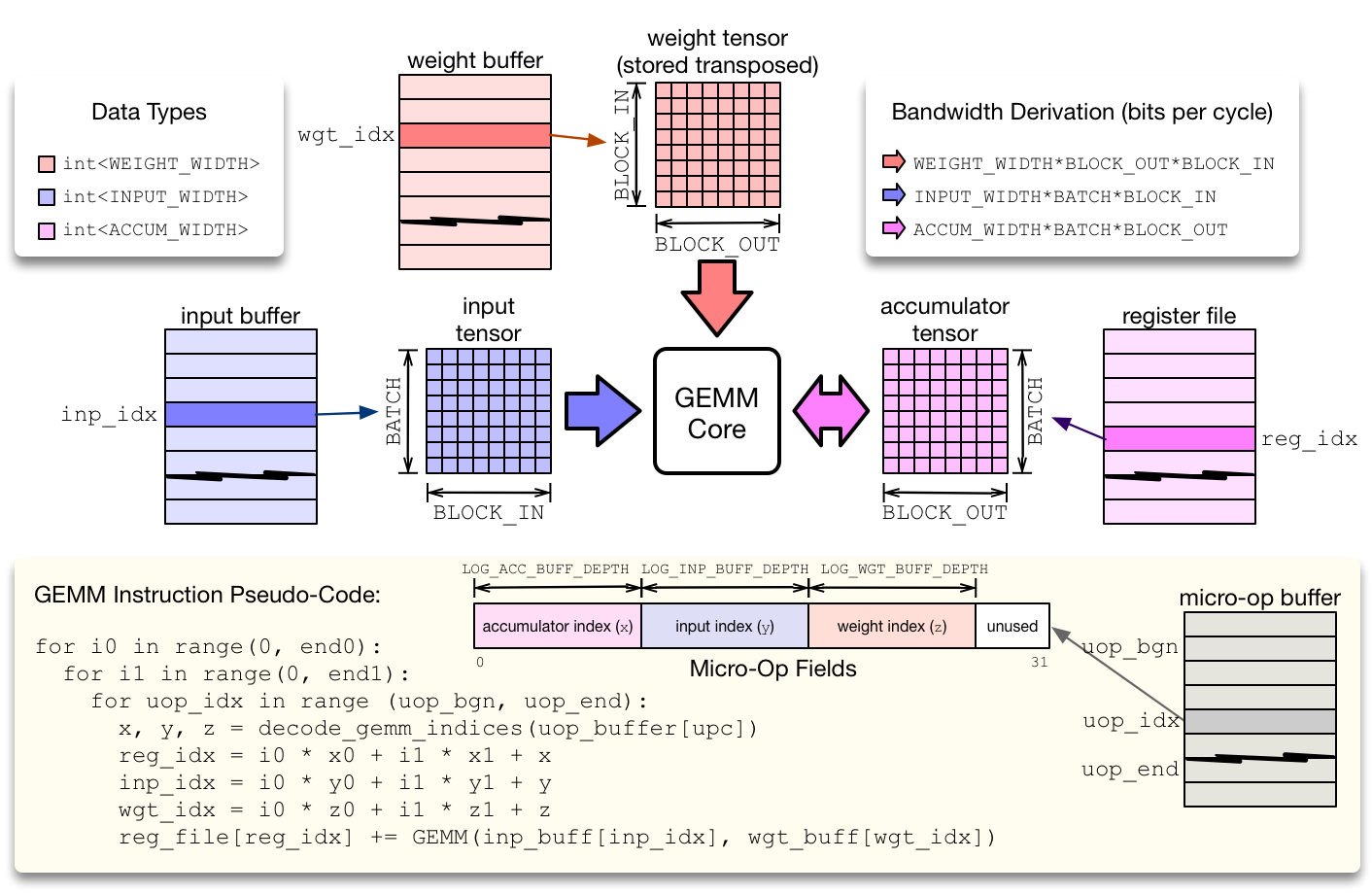
The GEMM core evaluates GEMM instructions, by executing a micro-code sequence in a 2-level nested loop described in the Figure above. The GEMM core can perform one input-weight matrix multiplication per cycle. The dimensions of the single-cycle matrix multiplication defines a hardware tensorization intrinsic which the TVM compiler has to lower a computation schedule onto. This tensorization intrinsic is defined by the dimensions of the input, weight and accumulator tensors. Each data type can have a different integer precision: typically both weight and input types are low-precision (8-bits or less), while the accumulator tensor has a wider type to prevent overflows (32-bits). In order to keep the GEMM core busy, each of the input buffer, weight buffer, and register file have to expose sufficient read/write bandwidth.
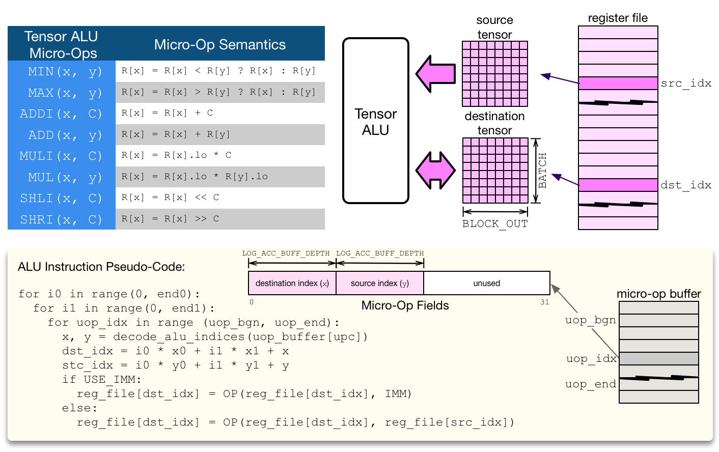
The Tensor ALU supports a set of standard operations to implement common activation, normalization, and pooling operators. VTA being a modular design, the range of operators that the Tensor ALU supports can be extended for higher operator coverage, at the expense of higher resource utilization. The Tensor ALU can perform tensor-tensor operations, as well as tensor-scalar operations on an immediate value. The opcode of the tensor ALU, and the immediate value are specified by the high-level CISC instruction. The micro-code in the context of tensor ALU computation only takes care of specifying data access patterns.
Note
In terms of computational throughput, the Tensor ALU does not execute at a rate of one operation per cycle. The limitation comes from the lack of read-ports: since one register file tensor can be read per cycle, the tensor ALU has an initiation interval of at least 2 (i.e. performs at most 1 operation every 2 cycles). In addition, performing a single tensor-tensor operation at once can be expensive especially given that register file types are wide, typically 32-bit integers. As a result, in order to balance the resource utilization footprint of the Tensor ALU with the GEMM core, a tensor-tensor operation is by default performed via vector-vector operations over multiple cycles.
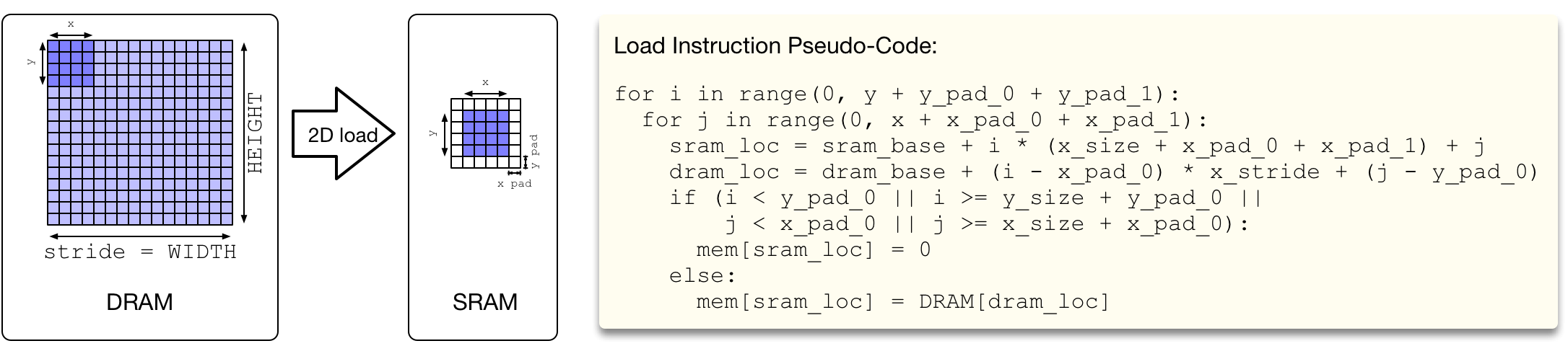
Load and Store Modules
The load and store modules perform 2D DMA loads with a strided access pattern from DRAM to SRAM. In addition, the load module can insert 2D padding on the fly, which is useful when blocking 2D convolution. This means that VTA can tile 2D convolution inputs without paying the overhead of re-laying data out in DRAM to insert spatial padding around input and weight tiles.